Good afternoon friends!
Recently, you and I have begun to get more closely acquainted with how computer hardware works. And we met one of his "bricks" - a semiconductor diode. is a complex system consisting of separate parts. By understanding how these individual parts (large and small) work, we gain knowledge.
Gaining knowledge, we get a chance to help our iron friend-computer if he suddenly goes haywire. After all, we are responsible for those we have tamed, aren't we?
Today we will continue this interesting business, and try to figure out how the most, perhaps, the main “brick” of electronics, the transistor, works. Of all the types of transistors (there are many of them), we will now limit ourselves to considering the operation of field-effect transistors.
Why is the transistor a field effect transistor?
The word "transistor" is formed from two English words translate and resistor, that is, in other words, it is a resistance converter.
Among the variety of transistors, there are also field-effect transistors, i.e. those that are controlled by an electric field.
The electric field is created by voltage. Thus, a field effect transistor is a voltage-controlled semiconductor device.
In English literature, the term MOSFET (MOS Field Effect Transistor) is used. There are other types of semiconductor transistors, in particular bipolar ones, which are controlled by current. In this case, some power is also spent on control, since a certain voltage must be applied to the input electrodes.
The FET channel can only be opened by voltage, with no current flowing through the input electrodes (except for a very small leakage current). Those. control power is not used. In practice, however, field-effect transistors are used for the most part not in a static mode, but are switched at a certain frequency.
The design of the field-effect transistor determines the presence of an internal transient capacitance in it, through which, when switching, a certain current flows, depending on the frequency (the higher the frequency, the greater the current). So, strictly speaking, some control power is still spent.
Where are field effect transistors used?
 The current level of technology makes it possible to make the open channel resistance of a powerful field-effect transistor (FET) sufficiently small - in a few hundredths or thousandths of an ohm!
And this is a great advantage, since even with a current of ten amperes, the power dissipated in the FET will not exceed tenths or hundredths of a watt.
Thus, bulky radiators can be abandoned or their dimensions can be greatly reduced.
FETs are widely used in computer and low-voltage switching regulators for computers.
From the whole variety of types of FETs, FETs with an induced channel are used for these purposes.
How does a field effect transistor work?
FET with induced channel contains three electrodes - source (source), drain (drain), and gate (gate).
 The principle of operation of the PT is half clear from the graphic designation and the name of the electrodes.
The PT channel is a “water pipe” into which “water” (a stream of charged particles that form an electric current) flows through a “source” (source).
"Water" flows from the other end of the "pipe" through the "drain" (drain). A gate is a "faucet" that opens or closes the flow. In order for the "water" to go through the "pipe", it is necessary to create "pressure" in it, i.e. apply voltage between drain and source.
If no voltage is applied (“no pressure in the system”), there will be no current in the channel.
 If a voltage is applied, then "open the tap" can be applied by applying voltage to the gate relative to the source.
The more voltage is applied, the more the “tap” is open, the more current is in the “drain-source” channel and the less is the channel resistance.
In power supplies, the FET is used in the key mode, i.e. the channel is either completely open or completely closed.
To be honest, the principles of the PT are much more complex, it can work not only in key mode. His work is described by many abstruse formulas, but we will not describe all this here, but will confine ourselves to these simple analogies.
We will only say that FETs can be with an n-channel (in this case, the current in the channel is created by negatively charged particles) and a p-channel (the current is created by positively charged particles). In the graphical image, for PTs with an n-channel, the arrow points inward, for PTs with a p-channel, it points outward.
Actually, a “pipe” is a piece of semiconductor (most often silicon) with impurities of various types of chemical elements, which determines the presence of positive or negative charges in the channel.
Now let's move on to practice and talk about
How to test a field effect transistor?
 Normally, the resistance between any FET terminals is infinitely large.
And, if the tester shows some slight resistance, then the PT is most likely broken and needs to be replaced.
Many FETs have a built-in diode between drain and source to protect the channel from reverse voltage (reverse polarity voltage).
Thus, if you put the “+” of the tester (red probe connected to the “red” input of the tester) to the source, and “-” (black probe connected to the black input of the tester) to the drain, then the channel will “ring”, like a regular diode in the forward direction.
 This is true for n-channel FETs. For p-channel FETs, the polarity of the probes will be reverse.
How to test a diode with a digital tester is described in the corresponding. Those. in the "drain - source" section, a voltage of 500-600 mV will drop.
If you change the polarity of the probes, a reverse voltage will be applied to the diode, it will be closed and the tester will fix this.
However, the health of the protective diode does not yet indicate the health of the transistor as a whole. Moreover, if you “ring” the PT without soldering it out of the circuit, then due to the parallel connected circuits, it is not always possible to draw an unambiguous conclusion even about the health of the protective diode.
In such cases, you can unsolder the transistor, and, using a small scheme for testing, unequivocally answer the question- whether the PT is working or not.
In the initial state, the button S1 is open, the voltage at the gate relative to the drain is zero. The PT is closed and the HL1 LED is off.
When the button is closed, a voltage drop (about 4 V) appears on the resistor R3, applied between the source and the gate. The PT opens and the HL1 LED lights up.
This circuit can be assembled as a module with a FET connector. Transistors in the D2 pack (which is designed for mounting on a printed circuit board) cannot be inserted into the connector, but you can insert conductors to its electrodes and insert them into the connector. To test the FET with a p-channel, the polarity of the power supply and the LED must be reversed.
Sometimes semiconductor devices fail violently, with pyrotechnic, smoke and light effects.
In this case, holes form on the case, it cracks or shatters into pieces. And you can make an unambiguous conclusion about their malfunction without resorting to devices.
In conclusion, we say that the letters MOS in the abbreviation MOSFET stand for Metal - Oxide - Semiconductor (metal - oxide - semiconductor). This is the structure of the FET - a metal gate ("faucet") is separated from the semiconductor channel by a layer of dielectric (silicon oxide).
I hope you figured out the “pipes”, “faucets” and other “plumbing” today.
However, theory, as you know, without practice is dead! It is necessary to experiment with field workers, dig deeper, tinker with checking them, feel, so to speak.
By the way, buy field effect transistors are possible.
Electronics surrounds us everywhere. But almost no one thinks about how this whole thing works. In fact, everything is quite simple. That is what we will try to show today. And let's start with such an important element as a transistor. We will tell you what it is, what it does, and how a transistor works.
What is a transistor?
Transistor- a semiconductor device designed to control electric current.
Where are transistors used? Yes, everywhere! Almost no modern electrical circuit can do without transistors. They are widely used in the production of computer technology, audio and video equipment.
Times when Soviet microcircuits were the largest in the world, have passed, and the size of modern transistors is very small. So, the smallest of the devices have a size of the order of a nanometer!
Console nano denotes a magnitude of the order of ten to the minus ninth power.
However, there are giant specimens that are used mainly in the fields of energy and industry.

There are different types of transistors: bipolar and polar, direct and reverse conduction. However, the operation of these devices is based on the same principle. A transistor is a semiconductor device. As is known, charge carriers in a semiconductor are electrons or holes.
The region with an excess of electrons is denoted by the letter n(negative), and the region with hole conductivity p(positive).
How does a transistor work?
To make everything very clear, consider the work bipolar transistor (the most popular type).
(hereinafter referred to as simply a transistor) is a semiconductor crystal (most often used silicon or germanium), divided into three zones with different electrical conductivity. Zones are named accordingly collector, base And emitter. The transistor device and its schematic representation are shown in the figure below.

Separate transistors of direct and reverse conductivity. P-n-p transistors are called forward-conducting transistors, and n-p-n transistors are called reverse ones.

Now about what are the two modes of operation of transistors. The very operation of the transistor is similar to the operation of a water tap or valve. Only instead of water - electric current. Two states of the transistor are possible - working (transistor open) and resting state (transistor closed).
What does it mean? When the transistor is closed, no current flows through it. In the open state, when a small control current is applied to the base, the transistor opens, and a large current begins to flow through the emitter-collector.
Physical processes in a transistor
And now more about why everything happens this way, that is, why the transistor opens and closes. Let's take a bipolar transistor. Let it be n-p-n transistor.
If you connect a power supply between the collector and emitter, the collector electrons will begin to be attracted to positive, but there will be no current between the collector and emitter. This is prevented by the base layer and the emitter layer itself.

If, however, an additional source is connected between the base and the emitter, electrons from the n region of the emitter will begin to penetrate into the region of the bases. As a result, the base region will be enriched with free electrons, some of which will recombine with holes, some will flow to the plus of the base, and some (most) will go to the collector.
Thus, the transistor turns open, and the emitter-collector current flows in it. If the base voltage is increased, the collector-emitter current will also increase. Moreover, with a small change in the control voltage, a significant increase in the current through the collector-emitter is observed. It is on this effect that the operation of transistors in amplifiers is based.

That's the whole point of how transistors work in a nutshell. Do you need to design a bipolar transistor power amplifier overnight, or do some lab work to study the operation of a transistor? This is not a problem even for a beginner, if you use the help of our student service specialists.
Feel free to seek professional help with important matters like studying! And now that you already have an idea about transistors, we invite you to relax and watch the video of the Korn band “Twisted transistor”! For example, you decide, contact the Correspondence.
For experience, we will take a simple and beloved KT815B transistor by all of us:
Let's assemble a familiar scheme:

Why did I put a resistor in front of the base, read.
On Bat1 I set the voltage to 2.5 volts. If you apply more than 2.5 volts, then the bulb will not burn brighter. Let's just say, this is the border, after which a further increase in the voltage at the base does not play any role on the current strength in the load

On Bat2, I set 6 Volts, although my light bulb is 12 Volts. At 12 volts, the transistor warmed up noticeably, and I did not want to burn it. Here we see how much current our light bulb consumes and we can even calculate the power it consumes by multiplying these two values.

Well, as you saw, the light is on and the circuit works fine:

But what happens if we mix up collector and emitter? Logically, our current should flow from the emitter to the collector, because we did not touch the base, and the collector and emitter consist of an N semiconductor.

But in practice, the light bulb does not want to burn.

Consumption on the Bat2 power supply is some 10 milliamps. This means that the current through the bulb still flows, but very weak.

Why does the current flow normally when the transistor is connected correctly, but not when connected incorrectly? The thing is, the transistor is not made symmetrical.

In transistors, the area of contact between the collector and the base is much larger than between the emitter and the base. Therefore, when electrons rush from the emitter to the collector, then almost all of them are “caught” by the collector, and when we confuse the leads, not all electrons from the collector are “caught” by the emitter.
By the way, miraculously, the P-N junction of the emitter-base did not break through, since the voltage was applied in reverse polarity. Parameter in datasheet U EB max. For this transistor, the critical voltage is considered to be 5 volts, but in our case it was even slightly higher:
So, we have learned that the collector and emitter unequal. If we confuse these conclusions in the circuit, then a breakdown of the emitter junction may occur and the transistor will fail. So, do not confuse the conclusions of the bipolar transistor in any case!
How to identify transistor pins
Method number 1
I think the easiest. Download datasheet for this transistor. In each normal datasheet there is a drawing with detailed inscriptions, where is which conclusion. To do this, we enter into Google or Yandex large numbers and letters that are written on a transistor, and add the word “datasheet” next to it. So far, there has not been such a thing that I did not look for a datasheet for some kind of radio element.
Method number 2
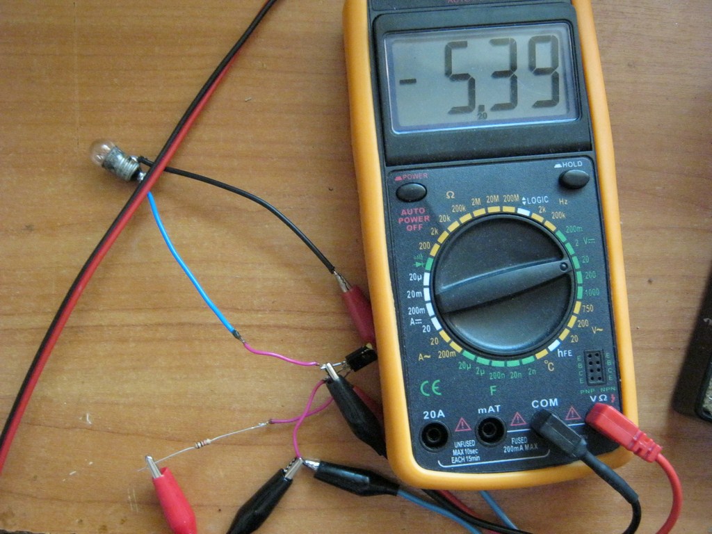
I think that there should be no problems with finding the base output, given that the transistor consists of two diodes connected in series either by cathodes or anodes:


Everything is simple here, put the multimeter on the dial icon “)))” and start trying all the variations until we find these two diodes. The conclusion where these diodes are connected either by anodes or cathodes is the base. To find the collector and emitter, we compare the voltage drop across these two diodes. Between collector and base ohm it should be less than between emitter and base. Let's check if it is?
First, consider the KT315B transistor:

E - emitter
K - collector
B - base
We put the multimeter on the dial and find the base without problems. Now we measure the voltage drop across both junctions. Base-emitter voltage drop 794 millivolts

The voltage drop across the collector-base is 785 millivolts. We have verified that the voltage drop between collector and base is less than that between emitter and base. Therefore, the middle blue terminal is the collector, and the red one on the left is the emitter.

Let's check the transistor KT805AM. Here is its pinout (pinout):

This is our NPN structure transistor. Suppose the base is found (red output). Find out where he has a collector, and where is an emitter.
We make the first stop.

Let's do a second check:

Therefore, the middle blue terminal is the collector, and the yellow one on the left is the emitter.
Let's check another transistor - KT814B. He is our PNP structure. Its base is a blue pin. We measure the voltage between the blue and red terminals:

and then between blue and yellow:

Wow! And there and there 720 millivolts.
This method did not help this transistor. Well, don't worry, there is a third way for this...
Method number 3
Almost every modern one has 6 small holes, and next to it there are some letters, something like NPN, PNP, E, C, B. These six tiny holes are just for measuring. I will call these holes holes. They don't look like holes.
We put the multimeter twist on the “h FE” icon.
We determine what conductivity it is, that is, NPN or PNP, and push it into such a section. Conductivity is determined by the location of the diodes in the transistor, if not forgotten. We take our transistor, which in both directions showed the same voltage drop at both P-N junctions, and stick the base into the hole where the letter “B” is.


We do not touch the base, but stupidly swap two conclusions. Opa-na, the cartoon showed much more than the first time. Therefore, hole E is currently the emitter, and hole C is the collector. Everything is elementary and simple ;-).

Method number 4
I think this is the easiest and most accurate way to check the pinout of a transistor. To do this, it is enough to purchase a Universal R / L / C / Transistor-metr and put the transistor leads into the device terminals:

It will immediately show you if your transistor is alive. And if he is alive, he will give out his pinout.


